There are very few electrical components that can boast of being at the core of most modern technology. From smartphones and laptops to medical imaging equipment, semiconductor diodes dominate the tech world, enabling the creation of wonders that would have seemed like impossible miracles a century ago. Interestingly the functioning of these diodes boils down to controlling the movement of just a few electrons through solid materials.
Why metals conduct
Most metals allow electricity to flow through them. To understand why, let’s delve into the atomic world and imagine any solid as a vast grid of atoms. Each atom is connected to its immediate neighbours through strong electrical forces. Each atom consists of a central positive nucleus surrounded by negatively charged electrons. In materials that don’t conduct electricity, known as insulators (such as wood and rubber) all the electrons are tightly bound to their atoms, leaving no freedom to move between them. Since electricity is the flow of electric charge, the absence of freely moving charges makes insulators non-conductors of electricity. However, in metals, the outermost electrons are loosely bound to the atom, requiring only a small amount of energy to free them. This allows these electrons to move between atoms, enabling the generation of an electric current.
Speaking of numbers, in a metal, each atom frees at least one of its outer electrons. Considering that even a tiny piece of metal is composed of billions and billions of atoms, you can imagine the vast number of free electrons available in metals. For instance, in magnesium, each atom contributes two electrons, so even a piece of the metal the size of a sugar cube has about 100,000,000,000,000,000,000,000 free electrons. This number consisting of 23 zeros surpasses the total number of sand grains on Earth by a factor of approximately 100,000. In essence, there are ample free electrons in metals that can flow to conduct electricity.
How're semiconductors different
While metals and insulators exhibit extreme differences in conductivity, with metals having high conductivity and insulators having nearly none, there exist materials known as semiconductors, such as silicon, whose conductivity lies somewhere in between. In semiconductors, all electrons are bound to their atoms at very low temperatures. However, at room temperature, due to the thermal vibrations of atoms, some outermost electrons gain enough energy to break free. This process is not possible in insulators because the energy required to free electrons is too high. The key advantage of semiconductors is that the energy required to free electrons is relatively low, making it possible for atomic vibrations at room temperature to produce free electrons. However, the number of electrons freed in this manner is significantly smaller compared to metals, being approximately a trillion times lower.
Despite their lower conductivity compared to metals, semiconductors play a crucial role in electronics. By strategically adding a few atoms of specific elements to a semiconductor (a process called doping), we can significantly enhance their conductivity and achieve a controlled flow of electrons—something nearly impossible with metallic conductors. For example, a piece of silicon the size of a sugar cube has about ten billion electrons at room temperature. By replacing just one silicon atom in five million with a phosphorus atom, we can increase the number of free electrons a million times.
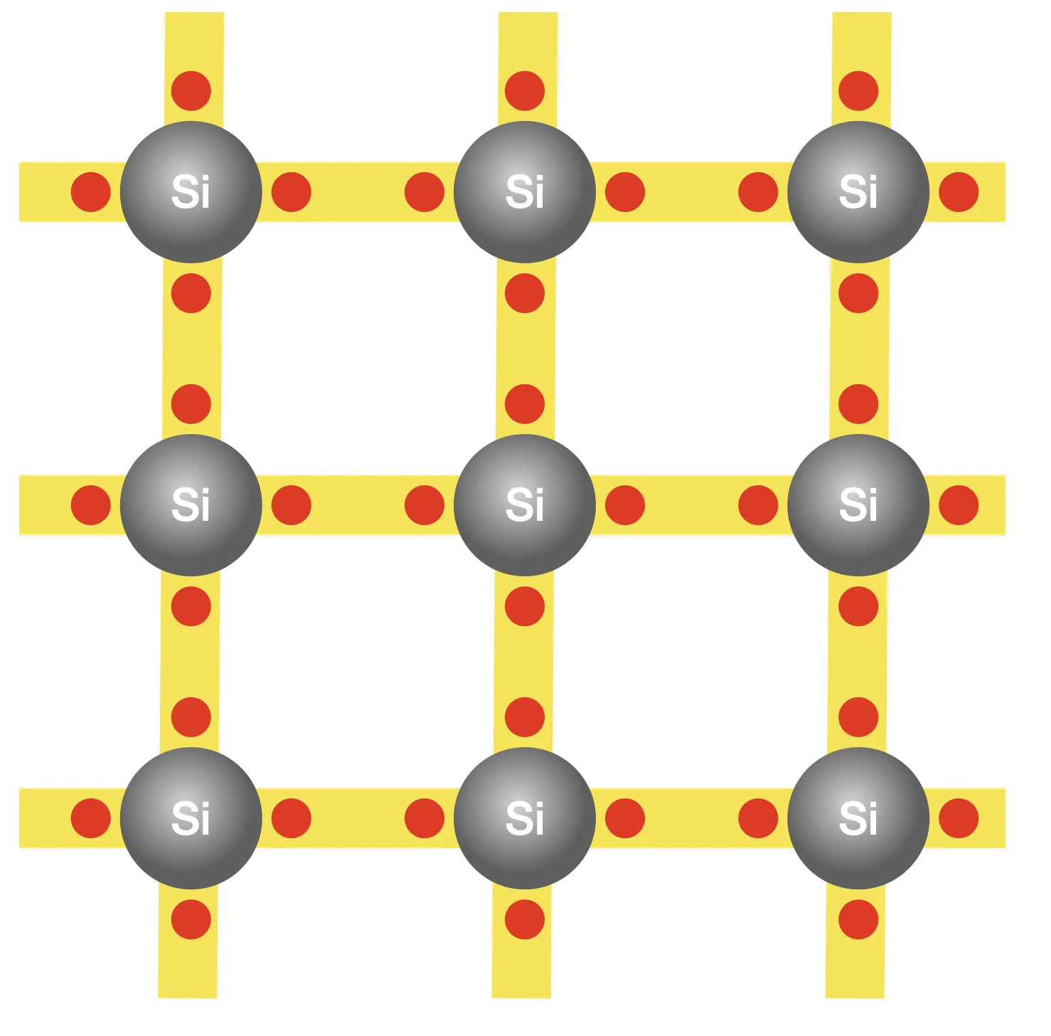
To understand the process, let’s examine the atomic structure of silicon. Each silicon atom has 14 electrons, with 10 occupying the inner core of the atom, leaving four electrons in the outermost parts. If only the atom possessed four additional electrons, it would have a lower energy and consequently greater stability. The atoms therefore adopt a strategy that involves each silicon atom sharing one of its outermost electrons with its four neighbouring atoms. This electron-sharing effectively enhances each atom’s outer electron count to eight, thereby minimizing atomic energies. The electron exchange between atoms creates a bond, enabling them to adhere to one another. And it is these bonds between the atoms that provides the solidity that characterizes a piece of silicon, shaping its structure.
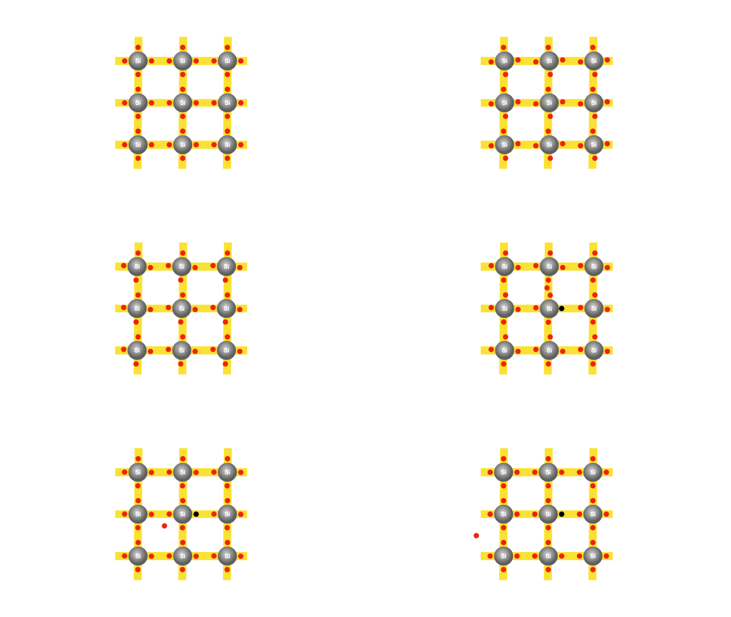
With the silicon atoms packed tightly, there appears to be no room for the existence of free electrons. In fact, at the lowest temperatures, a semiconductor becomes an insulator. However, at room temperature, as mentioned earlier, the silicon atoms vibrate with sufficient energy to cause a few electrons to gain enough energy and break free from their atoms. So that when a voltage is applied, these freed electrons can flow and constitute an electric current. Interestingly, each freed electron leaves behind an empty spot called a hole in the atom. The creation of the hole grants the bound electrons some freedom to move.
The need for doping
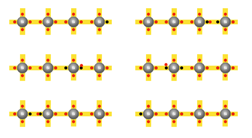
Imagine one of the bound electrons that initially had no mobility, now can move by occupying the hole, leaving one in its previous position for other electrons to hop into. As the electrons continue hopping into the created holes, it creates the illusion of the hole itself moving in the opposite direction. Therefore, for every freed electron, a hole is created, and the movement of both contributes to the conductivity of silicon. However, as discussed earlier, the conductivity of silicon is still too poor for practical use in electronics. That’s why we must consider replacing some of the silicon atoms with atoms of another element, such as phosphorus, that would provide additional free charges.
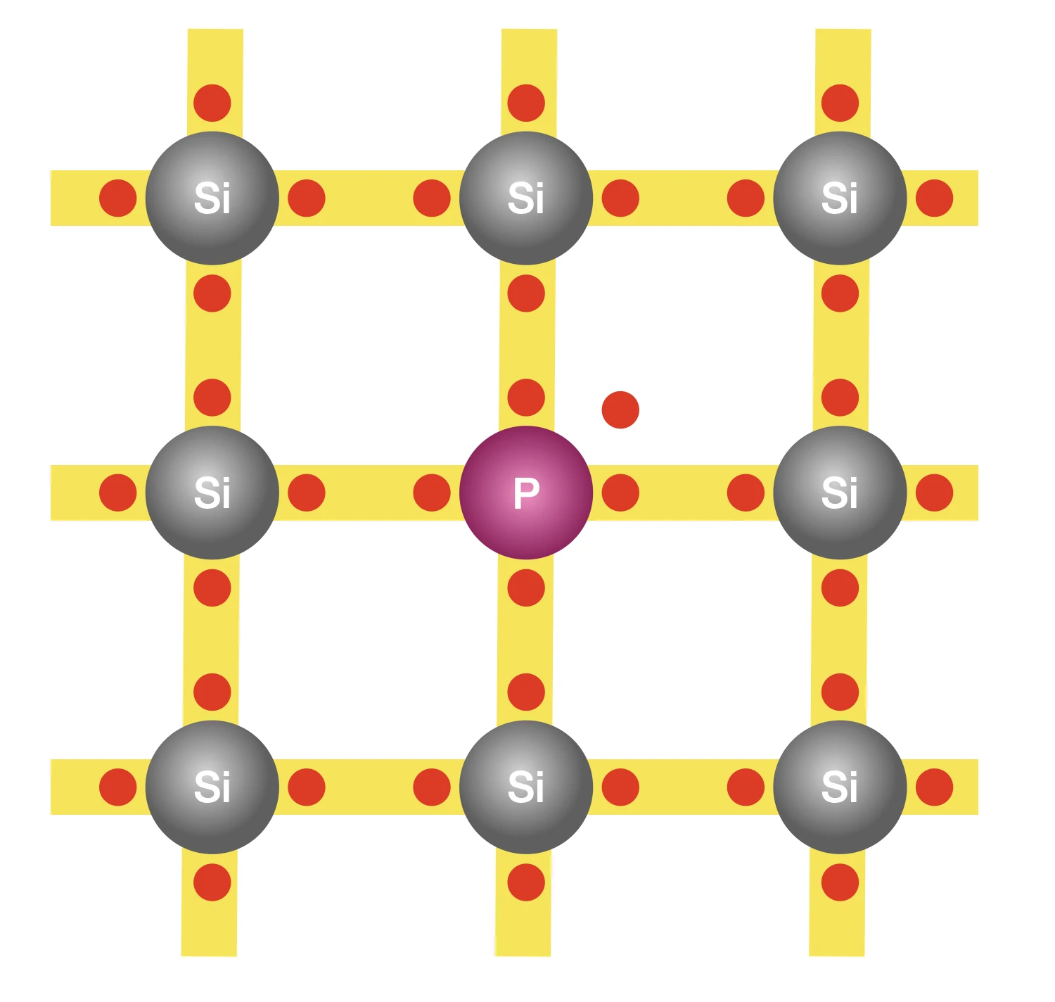
The process of doping involves adding suitable foreign atoms, such as phosphorus, to silicon. It is sufficient to replace just one in five million silicon atoms with a phosphorus atom. Recall that each silicon atom has four outer electrons; phosphorus on the other hand has five. Four of these electrons are used for bonding with the four neighbouring silicon atoms, leaving the fifth electron free to move. Hence, adding each phosphorus atom to the silicon base yields an additional free electron. And these free electrons aren’t generated by atomic vibrations, so no new holes are created in the process.
With sufficient phosphorus atoms added to the silicon base, we’ve created an excess of free electrons. While a holes do still exist due to freeing of electrons by atomic vibrations, they form a very small fraction of the number of free electrons. This type of a semiconductor is known as an n-type, where ’n’ represents negative, signifying the presence of excess free electrons which are negatively charged.
At this point, you might wonder why would we start with a semiconductor and then dope it to enhance its conductivity instead of directly using metals that have very high conductivity? The purpose of doping a semiconductor isn’t to make it as good a conductor as metals but instead to only slightly improve its conductivity so that when a voltage is applied, there is a flow of charge. That’s why we replace only one in five million silicon atoms with phosphorus atoms, not more. Our goal is to preserve all the semiconductors’ properties while tweaking their conductivity through doping.
The p-type
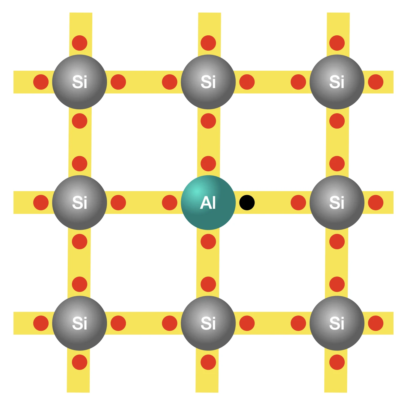
What makes semiconductors more intriguing is that by choosing to use aluminum atoms instead of phosphorus, for doping, we can create an excess of holes in the same silicon base. An aluminum atom has only three outer electrons, all of which are used to bond with the three neighbouring silicon atoms. This leaves an empty spot, a hole, in the aluminum atom that an electron can hop in, causing the hole to appear elsewhere. Amidst all the hoping of electrons, the number of holes remains significantly larger than the number of free electrons that could only have been created due to atomic vibrations. This type of semiconductor is known as a p-type, where ‘p’ represents positive.
It’s interesting to observe that while an excess of electrons results in an overall negative charge, an excess of holes leads to a net positive charge. A hole is not a positively charged particle; it’s an empty slot waiting to be filled by an electron. But if electrons are made to move in a certain direction by applying a voltage, say, they’d go on filling the holes in that direction, creating an illusion as though the holes are moving in the opposite direction, similar to how a positively charged particle would behave. Hence, it does no harm to imagine holes as positively charged particles, as long as you keep in mind that they aren’t but only move as if they were.
The p-type and n-type semiconductors, aren’t particularly useful on their own, but become remarkably powerful when combined in specific ways. These combinations enable a controlled flow of electrons, a feat that metals alone could never accomplish, as we shall see in part-2 of this article.
If \(n_e\) is the number of electrons and \(n_h\) the number of holes, then in an n-type semiconductor, \[n_e \gg n_h\]
and in a p-type, we have \[n_h\gg n_e\]
In any case, the total number of charge carriers in a semiconductor equals \(n_e+n_h\).

